Transcription Lead of Electroforming Method
Overview
Maxell has Transcription Lead of Electroforming method (click here for more information on electroforming) for semiconductor packages such as diodes, power protection ICs, voltage regulators, and DC/DC converters.
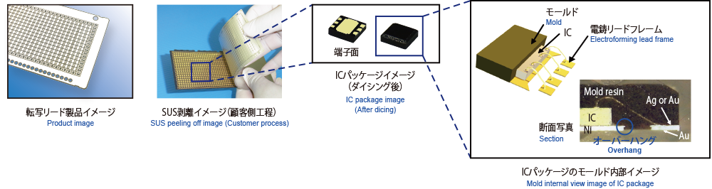
A lead frame is a thin metal substrate and Maxell's Transcription Lead frame is used only the electroformed part when making semiconductor packages compared to lead frames made by general stamping or etching methods. That’s why our lead frame can realize thinner semiconductor packages. (When packaging, user peel off our Transcription Lead frame from base material (SUS) which holds the pad)
In addition, since the metal connection between patterns is unnecessary structurally (isolated pad is possible), user can save the area for connection. As a result, more semiconductor packages can be assembled from a single substrate (higher integration) compared to a general lead frame substrate of the same size, which allows for improving design freedom and smaller semiconductor packages.
Our transcription Lead frame can be easily applied to small-volume, high-mix requirements, realize lower costs and shorter delivery times for initial prototypes.
Release:August 19,2021

Features
- Enables smaller and thinner semiconductor packages.
- Overhang solution at the top of the lead (structure to prevent peel off)
- Since the base material is metal, wobbling like that of general lead frames is suppressed, and excellent wire bonding.
- Unlike general lead frames, there are no metal connecting bars, which makes dicing faster and less blade wear, and also allows for higher package integration.
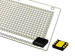
Image
Others
- IC mounting Achievement: paste, DAF (die attach film), FCB (flip chip), etc.
- Dicing: Individual pad formation possible = No metal cutting required
- SMT: Au plating enables SMT (including solder ball connection) without additional processing after dicing.
- Applications (examples): Voltage regulators, communication ICs, Li battery protection ICs, photo sensors, diodes, etc.
Specification
| Item | Specification |
|---|---|
| Pad thickness | Overhang: 65±15µm, Semi-overhang: 60±15µm |
| Au thickness | Min. 0.05µm |
| Ag thickness | Min. 2.0µm |
| SUS thickness | 150±10µm |
| Min. pitch from pad to pad | Overhang: Min. 200µm, Semi-overhang: Min. 150µm |
| Sheet size | 630×600mm (Effective area: 600×570mm) |
| Recommended strip size (example) | 190.0×57.5mm: 30 strips/sheet, 200.0×70.0mm: 24 strips/sheet, Max. strip size: 300.0×100.0mm |
| IC Package thickness (After molding) | Possible 0.3mm or less |
If you have further questions, please send us a message and one of our representatives will be in touch.
