Wafer Bumping Service
Overview
Maxell's Wafer Bumping Service is a processing service for the customer who need outsource solder ball bumping on various wafers with high reliability (small height variation and void suppression). UBM processing (electrolytic plating / electroless plating), rewiring and bump formation are also available. We also sell stencil for solder ball bumping using our electroforming technology. By using our metal stencil, we are also developing solder ball bumping with a diameter of 20µm or less. Please feel free to contact us for anything from small lot prototyping to mass production.
Release: August 19, 2021

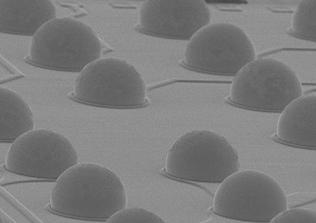
By using our metal mask with electroforming technology that we have built up for many years, it is possible to bump solder balls (Φ100µm or less) on wafers and form high-precision solder bumps. The method is good at void less bumping so we can achieve high coplanarity.
- wafer size: 6, 8 inches (Si, SiC, sapphire, glass, compound semiconductor)
- Ball diameter: 50µm or less
- MOQ: From 1 wafer for prototyping and mass production
- Bumping method: Transfer method (using a stencil to bump solder balls at a appropriated position)
- UBM (under barrier metal) processing: Electrolytic plating and electroless plating both available
- Insulating layer processing: Insulating layer processing using organic protective film (PBO) also available
- Back-end process: Back-grinding, laser marking, dicing, tape-packing, etc. are also available at partner companies
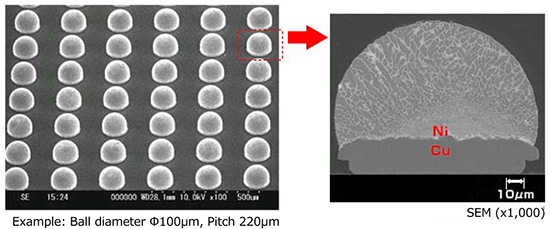
Image of Wafer Bumping Service
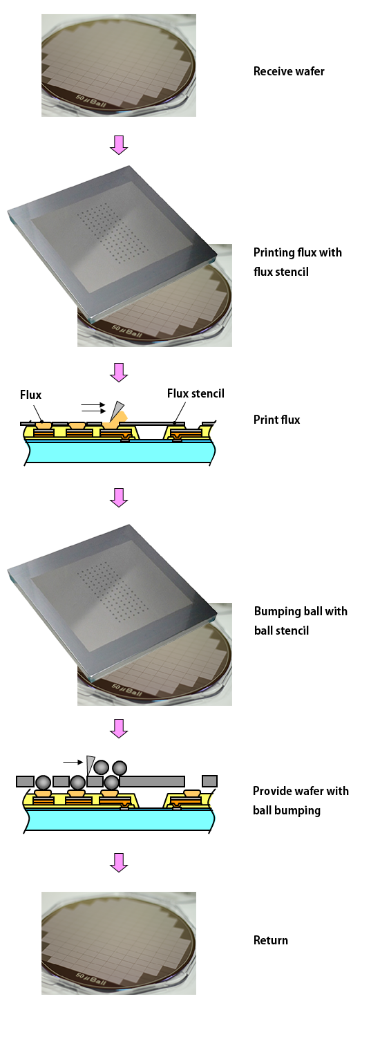
- We can provide only stencil for printing and solder ball bumping.
- Processing of electrolytic UBM and electroless UBM is also available.
- Only Sputtering on wafers is available as well.
- If you have further questions, please send us a message and one of our representatives will be in touch.
