TLEM (Transcription Lead of Electro-forming Method) technology introduction
What is TLEM?
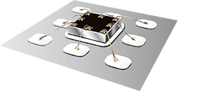
Electroformed lead frame that enables the miniaturization and thinning of IC packages (electronic components).
Patterns are formed by electroforming on a rigid SUS substrate, and patterns are transferred when ic packages (electronic components) are manufactured.
Low-volume multi-productmanufacturing. Ex. diodes, power protection ICs, voltage regulators, DC/DC converters, etc. use in Japan and overseas.
Do you have any problems designing and manufacturing electronic components?
- Improve the thickness of electronic components thinner.
- Design lead frames (e.g. LF-MAP) more quickly and easily.
- Reduce assembly costs.
- Shorten the time to completion of the sample.
<SOLUTION> TLEM can be achieved
(1) Improve design flexibility
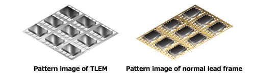
The connection between the patterns required in the lead frame is unnecessary for the TLEM. Free pattern design without considering the connection position is available.
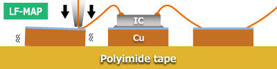
(2) Thinning of IC packages (electronic components)
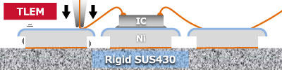
Thinning of the lead part can achieve low thickness of 0.3 mm or less.
(3) Assembly cost reduction
Pattern design is formed directly on the SUS substrate so individual pads can be formed.
= No metal cutting required (SUS cut type is also possible depending on design) ⇒ Improve dicing speed and reduce blade wear
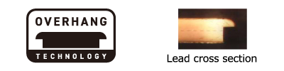
(4) Improve assembly yield
SUS with high rigidity is used for the substrate, so it is difficult to deform in the wire bonding process, and good wire bondability.
Overhang structure improves resistance to terminal omissions during molding process.
∗Overhang structure
(5) Manufacturing cost
Design cost: No frame connection is required because patterns are formed directly on SUS substrates.
Total cost: IC package (electronic components) size gets smaller and smaller, manufacturing cost per package is reduced.
(6) Contributing to the reduction of environmental impact
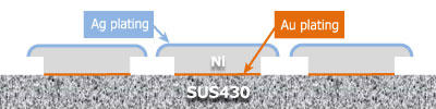
TLEM has a three-layer structure of Au/Ni/Ag (basic spec), the post plating process is unnecessary in customer process, and the environmental impact when manufacturing IC packages (electronic components) is reduced.
(7) Quick delivery (Samples)
Shortest delivery time: 25 working days (about 5 weeks)
∗1 Standard specifications only
∗2 After agreeing to specifications and receiving an order
∗3 Delivery time may be changed depending on the production situation after receiving an order
How to use TLEM
Packaging (customer process)
(1) Frame delivery (Spec:Au/Ni/Ag)
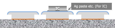
(2) Die bonding
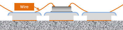
(3) Wire bonding
- SUS with high rigidity is used for the substrate so it is difficult to deform in the wire bonding process, and good wire bondability.
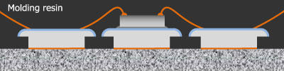
(4) Molding
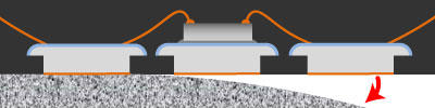
(5) SUS peeling
- Simple process of peeling the SUS substrate after sealing the resin
- There is Au plating after peeling, post-plating processing is unnecessary
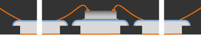
(6) Dicing (PKG singulation)
- Depending on the design, metal pattern cutting is not required, improving dicing speed and reducing blade wear

(7) Packaging completed
Product information
Please check the TLEM web page about products, specifications and flyer.
OVERHANG(Japan Registered Trademark No.5883494)and TLEM(Japan Registered Trademark No.5933307)are registered trademarks of maxell.
OVERHANG logos are trademarks of maxell.
The names, logos, and service marks mentioned herein are registered trademarks or trademarks of other companies.
Release: October 26, 2021
