Test wafer
Summary
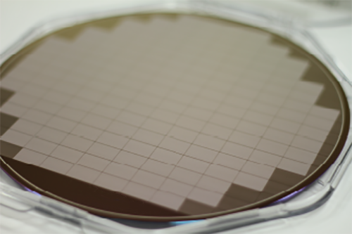
Maxell have test wafers with solder bumps (evaluation wafers with solder balls already bumped) for use in the evaluation of materials and equipment for semiconductor processes.
Test wafers could be made with unique patterns (custom products) for each customer, which resulted in relatively high initial costs for small-quantity procurement and a heavy burden for customers.
Maxell has met these customers demand by providing test wafers with a predetermined pattern*1 as a standard product at a reasonable cost, making it possible to provide test wafers with as little burden as possible to customers.
It can be used in a wide range of customer research and development processes, such as back grinding and dicing processes.
*1: Customer-specific patterns are also available upon request at an additional initial cost.
Release: August 19, 2021

Features
- The price can be reduced by using standardized patterns.
- Non-standard specifications are available depend on initial cost (with or without solder bumps, layout changes such as bump diameter and pitch are also possible).
MOQ is 25pcs. If you have further questions, please send us a message and one of our representatives will be in touch.
Image
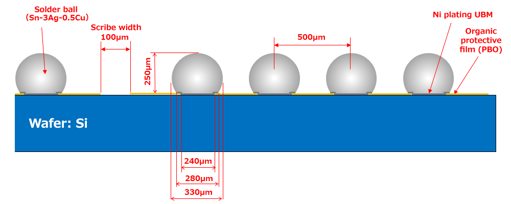
Standardized patterns (bump height 250µm)
| Item | Target figure |
|---|---|
| Chip pitch | 2,000µm |
| Scribe width | 100µm |
| Organic protective film thickness | 4µm |
| Organic protective film diameter | 240µm |
| Ni Plating UBM diameter | 280µm |
| Bump height | 250µm |
| Bump solder ball diameter | 330µm |
| Bump pitch | 500µm |
| Bump form area | Φ193mm |
| Wafer diameter | Φ200ミmm |
| Wafer thickness | 725µm |
