Stencil: For printing and solder ball bumping
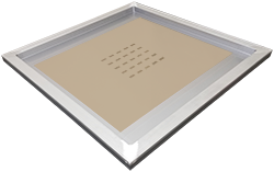
Stencil for Flux/Paste Printing
Our photolithography technology realizes excellent vertical cross-sectional shape and high-precision hole dimensions of ±3µm (depending on conditions). It is also possible to form aperture that are smaller than the thickness.
We have various surface treatment solutions: besides we can control thickness. We can also propose a 3D structure for printing stencils, such as for bumping solder balls, which enables printing with less damage to the substrate. our electroforming technology achieves a high hardness of approximately HV500.
Stencil for bumping solder balls
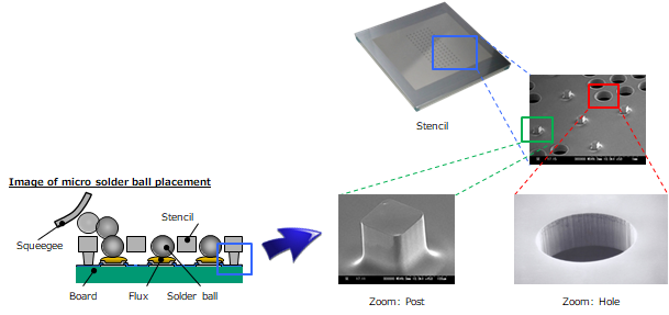
Our stencil has a special post structure to enable one-time mounting of solder balls and can bump solder balls with Φ50µm or more in mass production. (30µm or more is also possible in prototyping). In addition, by ensuring the flatness of the stencil, an excellent bumping yield rate is achieved compared to general solder ball bumping stencils (two layer electroforming structure).
In addition to the metal post, we also have resin post for bumping solder balls to meet customer needs.

Specification
| Metal size | Effective area | Pitch (mass production) | Thickness | |
|---|---|---|---|---|
| Flux/Solder paste stencil | Max. 550×550mm | 350×350mm | Min. 90µm | Min. 15µm |
| Solder ball bumping stencil | Max. 550×636mm |
∗We have Φ30µm aperture stencil for prototyping
∗If you have further questions, please send us a message and one of our representatives will be in touch.


