Package Foundry
Summary
Package Foundry is a foundry service specializing in small volume manufacturing of FOWLP (Fan Out Wafer Level Package) and WLCSP (Wafer Level Chip Size Package).
We fabricate Cu rewiring packages utilizing semiconductor front-end process and plating technology. In addition to silicon, we also have experience in packaging compound semiconductors such as SiC and GaN.
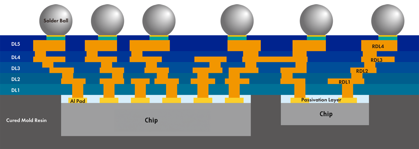
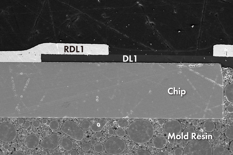
RDL: ReDistribution Layer
DL: Dielectric Layer
Release:May 31,2024

Delivery time and Price
There is no need to supply wafers in units as we can make solder bump on chips that diced into small pieces. We may offer competitive prices and shorter delivery times compared to overseas OSATs and semiconductor laboratories.
Design and Verification
PoC of the designed chips by package with rewiring (RDL). Functional verification of heterogeneous packages (SiP) that combine multiple chips with different functions.
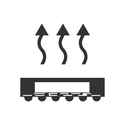
Heat dissipation
No package substrate or bumps are required, enabling a low profile package. The lower profile can be expected to reduce thermal resistance and improve heat dissipation.
Process integration
We help our customers solve their problems by integrating wafer front-end process, packaging process, and plating process.
Package Structure Comparison
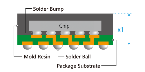
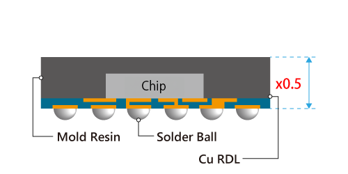
Package substrate, wire bonding, or solder bumps are not required for FOWLP structure, and it allows reducing size and profile in comparison with FCBGA structure.
Forming multi RDL on Al pad on chip by using both lithography and plating technology allows more flexible RDL design than conventional package.
Furthermore, the minimum package thickness of 100μm is possible.
Innovative Technology

Maxell's package foundry has 1 inch WLP production line specialized in prototype. PoC(Proof of Concept) of design can be done by a few packages in short period.
Evaluation of middle-volume and low-volume before production uses 6 inch line of same base line with 1 inch, so resetting condition is not required.
We develop various types of package as shown in following table, and we aim to continuously develop innovative technology upon the customer's need.
| Production Line | 1 or 6 inch production line (Prototype, High-mix Low-volume Production, Multi-layer RDL) |
|---|---|
| Package Type | FOWLP, WLCSP, SiP (System-in-Package), DSEP (Double-sided Electrode Package), AiP (Antenna-in-Package), Thin Package |
| Bump | Cu Pillar Bump, Cu Pad, Solder Bump |
Fan-Out Wafer Level Package (FOWLP)
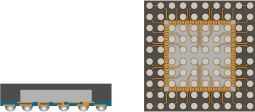
RDL interposer is connected to the input/output pads of the chip, and it allows connecting to any position on the board.
Heat dissipation can be expected to be improved due to muniaturization or lower profile.
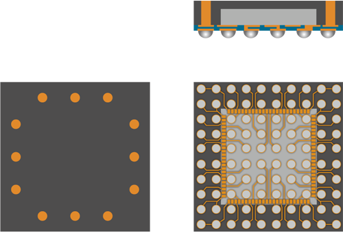
Wafer Level Chip Scale Package (WLCSP)
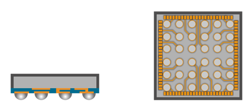
Package size of WLCSP is same as mounted chip.
Solder bumps can be formed on chips that is diced into small pieces by using shuttle service.
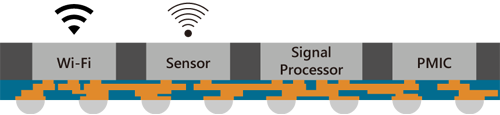
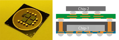
System in Package (SiP)
Systematization of multiple ICs with different functions in a single package make it high functionality and space saving in the package.
Power consumption is expected to reduce because mounting area becomes smaller.
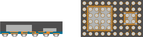
Double-sided Electrode Package (DSEP)
The I/O signals of the chip can be connected from the front side and back side of the package. High functionality can be achieved by stacking packages.
∗ Package on Package (Stacking IC Package) is not our business.
Thin Package
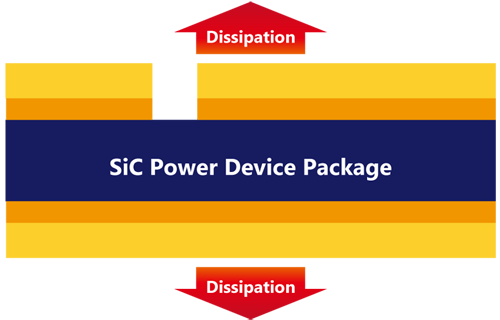
The package is made thinner to 100µm to facilitate heat dissipation and prevent heat retention inside the package.
This package is also suitable for wearable modules that ultra-thin shape is required, such as medical devices.
Antenna in Package (AiP)
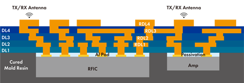
Utilize multi-layer RDLs to integrate the antenna structure into the package.
Conventionally, antenna element used to be connected separately. Anttena structure can be built in package by utilizing multi layer RDL, and this technology allows miniaturization of RF (high-frequency) device package.
Antenna shapes are available upon customer's requirement.
This technology can be applied to RF device more than several hundred GHz.
Cu Pillar Bump

In addition to Cu pad or solder bump, Cu pillar bump of dia.40μm x (t=)40μm can be formed.
In the midst of the growing need toward increasing number of terminals due to high-integration of package, this can meet the request of narrow pad pitch.
MRDL: Multi Redistribution Layer
FOWLP Process Flow
Our baseline process is face-down chip-first.
When you need face-up chip-first, RDL-first or other specific process options, please feel free to contact us.
STEP1 Reconstruction Wafer Process
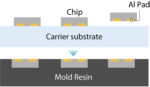
Rearranging chip on carrier substrate and curing with resin.
After that, peeling off carrier substrate.
STEP2 Redistribution Process
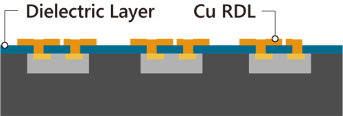
Constructing redistribution layer (RDL) by patterning dielectric layer (DL) and Cu RDL.
STEP3 Solder-ball Mounting Process
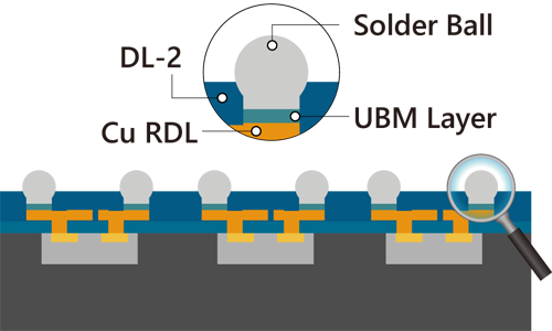
Constructing upper dielectric layer (DL-2) and UBM Layer, and mounting solder ball on it.
STEP4 Dicing Process

Deliver singulated package by dicing.
Design Rules
This is package structure incorporating chip or sensor.
Chips can be provided without solder bump. Both solder ball and Cu pad are available for external terminal in packages.
| Package Size | 1mm□∼20mm□ (Please contact us for sizes over 20mm x 20mm.) |
|---|---|
| Fan-Out Mold Resin Substrate | Size: Dia.22mm / 150mm |
| Dielectric Layer (DL) | Thickness: 4∼10μm |
| Cu Redistribution Layer (Cu RDL) | Layer Thickness: 3∼15μm Layer Number: Max. 4 Layers |
| Cu Redistribution L/S | Min. 20μm/20μm / via diameter:Min.Φ20μm (Please contact us for L/S and via diameters below 20μm.) |
| UBM | Material: Ni/Au |
| Solder Ball | Ball Dia.: 250∼500μm Pitch: ≧400μm |