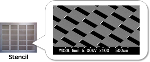
What is EF²?
Electroforming is an abbreviation of "electrocasting". Maxell calls it "EF2". This is an abbreviation of Maxell's precision electroforming technology "Electro-Fine-Forming".
Maxell - Electro-Fine-Forming (EF2) Technology
With the increasing miniaturization and high functionality of electronic devices, precision processing technology required for electronic components is becoming an increasingly important factor in the high-tech industry. In particular, the demand for higher precision and high-density mounting of components is increasing due to the high-density integration of semiconductors that require high precision and quality, and the expansion of small electronic devices. Maxell's electroforming (EF2: Electro-Fine-Forming) was developed as a technology for miniaturization and high functionality. In the future, electroforming is expected to have a key role as a key factor in new technological innovation in various fields, including precision electronic components. Maxell will continue to focus on development, design, and manufacturing.
Principle
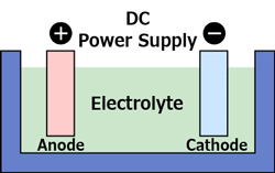
When the metal which is to be electroformed on the anode side is put into the sulfamic acid nickel liquid at a adequate temperature, allocate matrix such as stainless steel towards the cathode side and apply electronic current, the metal of the anode side gradually melt and form the patterns with the non conductor film on the surface of matrix that become apertures.
Difference between electroforming and plating
Electroforming process image
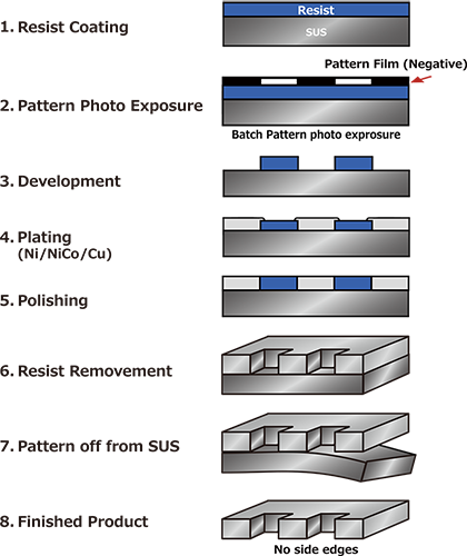
Electroforming is a technology in which a non-conductor film is installed as necessary, electrolytic plating is performed on the surface of the conductor, and then peeled off from the conductor to make a product to obtain the desired shape.
Plating is performed to give a function (Decoration, Reliability∗, etc.) to the surface of an object, and is integrated with the object as a product.
∗Reliability: corrosion resistance, connectivity, wettability
Performance cost comparison
| EF2 | Etching | Laser | |
|---|---|---|---|
| Materials | Mainly Ni·Cu (Au·Ag) | All materials which can corrode | Almost all materials |
| Aperture width (Aspect ratio) |
 (Max. 2) |
× Less than plate thickness are impossible |
○ (Depends on materials, a kind of the laser) |
| Aperture dimensional accuracy *In case of under 100µm plating thickness |
+/-3µm* |
× +/-10∼20µm* |
○ +/-5∼10µm* |
| Plating thickness accuracy | Thin product: |
Thin product (It is hard to obtain it.): △ | Thin product (It is hard to obtain it.): △ |
| Thick product: △ Approximately +/-5% of plate thickness (Depends on pattern) | Thick product: ○ Approximately +/-5% of plate thickness | Thick product: ○ Approximately +/-5% of plate thickness | |
| Cost | Thin product: Cheap Thick product: High |
Cheap | A price greatly changes (Depends on the number of the pattern) |
∗ Based on our own research
EF2 Advantages
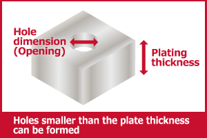
Hole formation is possible with an aspect ratio of 1:2
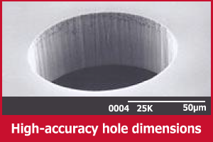
Depending on specifications ±1μm or less is possible
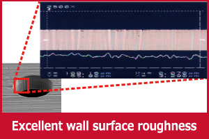
Ra(Surface roughness)=0.1μm
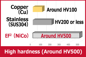
EF2 has a high hardness of around HV500
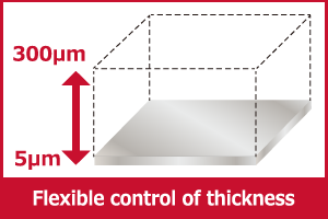
Min.5μm∼Max.300μm
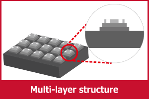
Multi-layer structure is possible to repeat photolithography and plating process
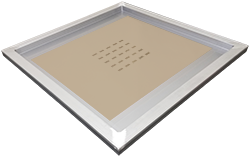
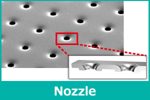
Semiconductor related products
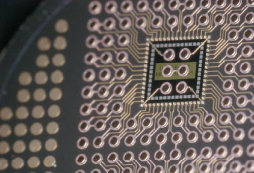
Electronic Components related products
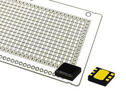
In addition, we also have optical slit plates for encoders, solder ball adsorption heads, precision positioning jigs, diffraction gratings, etc.
< Rule of thumb to apply EF² >
- Materials less than thickness 300µm that high dimensional accuracy is required by aperture width or rib width.
Production records other than those related to electronic components
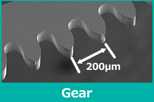
Durable with high hardness of around HV500 and can be manufactured with excellent accuracy
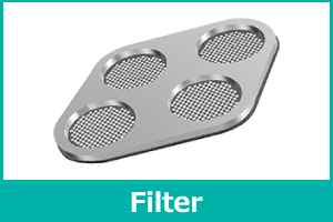
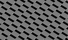
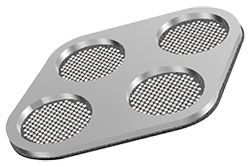
Flat mesh with high filtration accuracy can be manufactured
Specially shaped openings can be formed
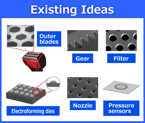
Expanding possibilities with Maxell's electroforming
Maxell's electroforming technology has been adopted mainly in the field of semiconductor components and electronic components, which are required miniaturization, high functionality, and high accuracy.
Maxell would like to continue to expand its lineup of electroforming products.
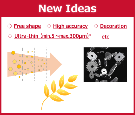
For example,
- Free shapes are formed by electroforming with ultra-thin (Min.5∼Max.300µm)∗ foil
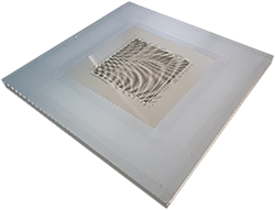
- Creating invisible high-precision shapes in μm size by stacking them by electroforming
- Stacking and creating beautiful formations using gold and silver electroforming
With free thinking, we aim to create new value for various applications and fields by utilizing our electroforming technology.
Please feel free to contact us if you have any problems or requests.
Possibilities of electroforming (EF2) technology
∗ Measurement using Mitutoyo Digimatic Indicator
