Tapes for semiconductor manufacturing process
Supporting Semiconductor Manufacturing Processes with Diverse Products
With the recent miniaturization of various electronic devices and the growing demand for semiconductor chips, the needs for various process technologies are growing more and more. In addition, with the ultra-thin wafers brought about by technological innovation, the ability to respond to the back grinding and dicing processes is also in question. Maxell offers solutions suitable for various processes, such as backgrinding and dicing, in the semi-conductor manufacturing process.
What is semiconductor?
A material that is intermediate between a conductor that conducts electricity well, such as metal, and an insulator that does not conduct electricity, such as rubber, under certain conditions (voltage, current, light, heat, etc.).
Typical examples include silicon (Si) and germanium (Ge), and for compounds gallium arsenide (GaAs).
At present, IC (integrated circuits) using these materials are also commonly referred to as semiconductors.
Semiconductor manufacturing process
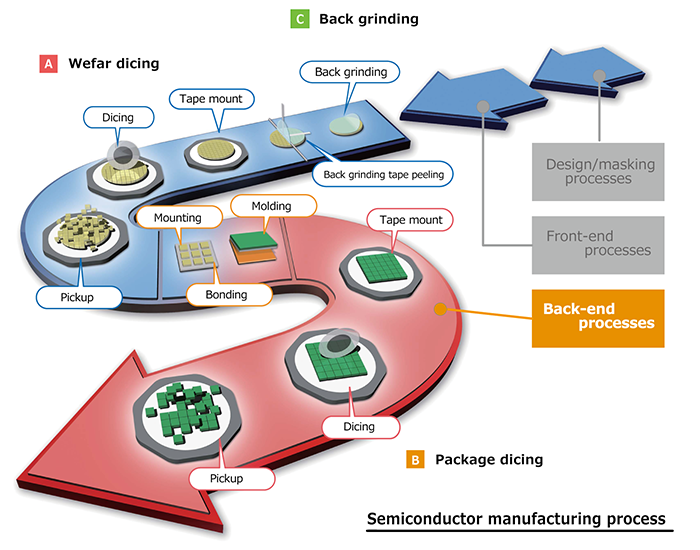
The semiconductor manufacturing process is broadly divided into the following three categories.
- Design process: Design of circuits and patterns, creation of photomasks
- Front-end process: Creating a circuit in an actual wafer
- Back-end process: Assembly and processing of wafers created in the pre-process as devices
Maxell manufactures and sells tapes for semiconductor-manufacturing processes, such as backgrind∗1, wafer dicing∗2, and package dicing∗3, which are mainly conducted in 3).
- This process grinds the backside thinly while protecting the surface (circuit-forming surface) of the wafer.
- The process of singulating thinned wafers into chips. Cutting them into squares like a die (Dice) is called dicing (Dicing).
- This is a process in which chips connected and fixed to the board are sealed (packaged) collectively, and then packages are singulated.
【A】 Dicing Tape for Wafer
- We use UV release adhesive, which has less adhesive residue when stripping the tape.
- The use of a special UV peel-off pressure-sensitive adhesive makes it easy to peel off. When peeling off, the adhesive becomes weaker due to UV exposure.
- Special PO (Polyolefin) is used as the base film. It has isotropic elongation.
- The 10 substances regulated by the RoHS Directive are all below the regulatory values.
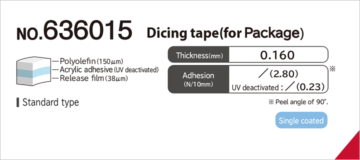
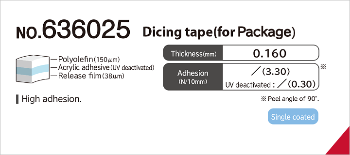
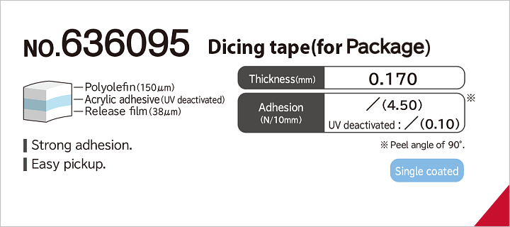
【B】 Dicing Tape for Package
- We use UV release adhesive, which has less adhesive residue when stripping the tape.
- The use of a special UV peel-off pressure-sensitive adhesive makes it easy to peel off. When peeling off, the adhesive becomes weaker due to UV exposure.
- Special PO (Polyolefin) is used as the base film. It has isotropic elongation.
- The 10 substances regulated by the RoHS Directive are all below the regulatory values.
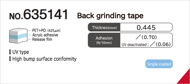
【C】 Back grinding tape
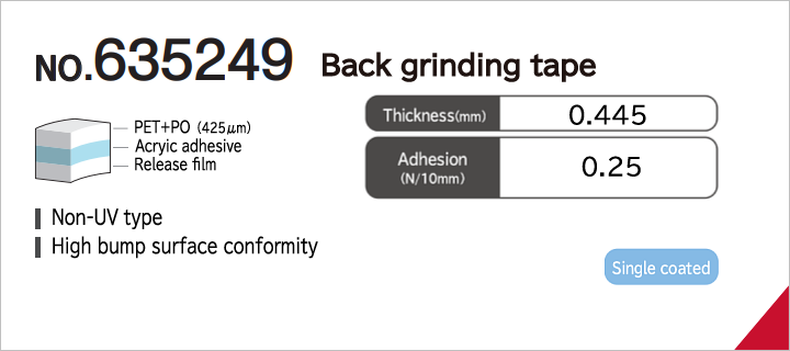
- Highly traceable to irregularities such as bumps on the wafer surface, preventing dimples and wafer damage after backgrinding.
- PET base material is used to prevent wafer warpage.
- Bump height of 100µm or more (approx.-300µm) is also available.
- Two types are available: UV peeling type and pressure sensitive type.
Description of adhesion
Our adhesion test is based on JIS Z 0237(2022).
For comparison to the conventional method, the tested value by Sliontec Method is also described in the parenthesis.
Please refer to the URL below for detail methods of JIS method and Sliontec method.
https://biz.maxell.com/en/sliontec_tapes/measuring_method.html

Product List
| Model | Product | Application | Features | Tape thickness | Adhesion | Coating |
|---|---|---|---|---|---|---|
| No.635141 | Back grinding tape | For various back grinding | UV type, High bump surface conformity | 0.445mm | Initial: 0.70N/10mm After UV:0.06N/10mm |
Single |
| No.635249 | Back grinding tape | For various back grinding | Non-UV type, High bump surface conformity | 0.445mm | 0.25N/10mm | Single |
| No.636000 | Dicing tape | For various wafer dicing | Standard type | 0.10mm | Initial: 2.80N/10mm After UV:0.23N/10mm |
Single |
| No.636020 | Dicing tape | For various wafer dicing | High fixing force | 0.10mm | Initial: 3.30N/10mm After UV:0.30N/10mm |
Single |
| No.636050 | Dicing tape | For various wafer dicing | Easy pick up | 0.10mm | Initial: 2.80N/10mm After UV:0.08N/10mm |
Single |
| No.636015 | Dicing tape | For various package dicing | Standard type | 0.16mm | Initial: 2.80N/10mm After UV:0.23N/10mm |
Single |
| No.636025 | Dicing tape | For various package dicing | High fixing force | 0.16mm | Initial: 3.30N/10mm After UV:0.30N/10mm |
Single |
| No.636055 | Dicing tape | For various package dicing | Easy pick up | 0.16mm | Initial: 3.00N/10mm After UV:0.10N/10mm |
Single |
| No.636095 | Dicing tape | For various package dicing | Easy pick up, Strong adhesion | 0.17mm | Initial: 4.50N/10mm After UV:0.10N/10mm |
Single |


