Transcription Lead of Electroforming Method

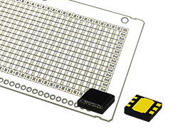
Electroformed lead frame that enables the miniaturization and thinning of IC packages (electronic components). Patterns are formed by electroforming on a rigid SUS substrate, and patterns are transferred when ic packages (electronic components) are manufactured. Low-volume multi-productmanufacturing. Ex. diodes, power protection ICs, voltage regulators, DC/DC converters, etc. use in Japan and overseas.

Lead frames produced by conventional etching methods typically involve the peeling of polyimide tape at the final stage of the customer process, resulting in waste. In contrast, Maxell's transfer leads have a stainless steel (SUS) substrate that is peeled off at the end, which can be reused, thereby contributing to waste reduction.
Additionally, lead frames made using etching methods may require a cleaning process to remove adhesive residues after the polyimide tape is removed. However, transfer leads do not have any adhesive between the SUS and the electroformed parts, eliminating the need for cleaning after SUS peeling (no cleaning agents are necessary).
Compared to etching-based lead frames, transfer leads allow for thinner packaging and a higher number of packages per frame. This results in reduced amounts of molding resin used per package. For instance, assuming a package size of 0.6 × 0.3 mm, our estimates suggest that the number of transfer lead packages per frame is about twice that of etching-produced lead frames, potentially reducing the amount of molding resin used by approximately half.
Furthermore, since etching lead frames involve dissolving materials to form patterns during production, they require waste liquid treatment. In contrast, transfer leads form patterns only where needed through electroforming, enabling waste reduction and material reuse, thus contributing to environmental considerations both in the customer process and in the production process of the lead frames.
∗ Research by Maxell
- Waste reduction is possible as polyimide tape is not used (the peeled SUS substrate can be reused).
- The need for a cleaning process to remove adhesive residues after peeling polyimide tape is eliminated.
- The use of molding resin can be reduced due to thinner packaging and an increased number of packages per frame.
- In the production process, patterns are formed only where necessary through electroforming, enabling waste reduction and material reuse.
Contributing to Customer's Environmental Impact Reduction
Transfer leads feature a three-layer structure of Au/Ni/Ag (basic specifications), which eliminates the need for an additional plating process in customer manufacturing. This contributes to the reduction of environmental impact during the production of IC packages (electronic components).

Related Information