FOWLP (Fan-Out Wafer Level Package)

Package Foundry is a foundry service specializing in small volume manufacturing of FOWLP (Fan Out Wafer Level Package) and WLCSP (Wafer Level Chip Size Package).
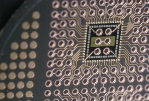
We fabricate Cu rewiring packages utilizing semiconductor front-end process and plating technology. In addition to silicon, we also have experience in packaging compound semiconductors such as SiC and GaN.
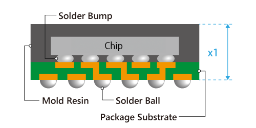
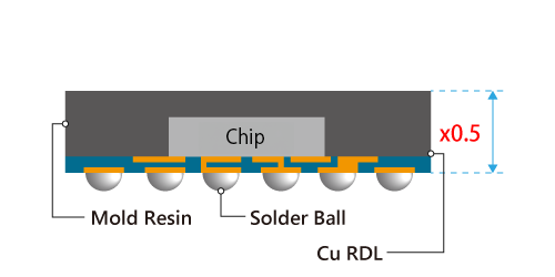
Package substrate, wire bonding, or solder bumps are not required for FOWLP structure, and it allows reducing size and profile in comparison with FCBGA structure.
Forming multi RDL on Al pad on chip by using both lithography and plating technology allows more flexible RDL design than conventional package. Furthermore, the minimum package thickness of 100μm is possible.
By integrating different functions onto a single chip in a wafer state, and then connecting individual chips for packaging (FOWLP) over short distances, we contribute to improving the yield during chip manufacturing. Furthermore, by positioning chips with different functions close together and connecting them using plated wiring, we can reduce the wiring length between chips, as well as the materials used, such as molding resin, to less than half, compared to traditional individual semiconductor package assembly.
∗ Research by Maxell


Related Information